-
Applied Materials Breakthrough in Electron Beam Imaging Technology Accelerates Development of the World’s Most Advanced Computer Chips
المصدر: Nasdaq GlobeNewswire / 14 ديسمبر 2022 04:30:51 America/Los_Angeles
- Applied’s new “cold field emission” technology works at room temperature, increasing nanoscale image resolution by up to 50% and imaging speed by up to 10X
- CFE eBeam technology enables leading chipmakers to accelerate development and commercialization of emerging 3D Gate-All-Around logic transistors and next-generation DRAM and NAND memory chips
- Two new CFE eBeam products introduced – SEMVision® G10 for defect review and PrimeVision® 10 for defect inspection – extending Applied’s leadership in the eBeam process diagnostics and control market
SANTA CLARA, Calif., Dec. 14, 2022 (GLOBE NEWSWIRE) -- Applied Materials, Inc. today announced the commercial availability of “cold field emission” (CFE) technology, a breakthough in eBeam imaging that enables customers to better detect and image nanometer-scale, buried defects to speed the development and production of next-generation Gate-All-Around (GAA) logic chips as well as higher-density DRAM and 3D NAND memories.
Chipmakers use eBeam technology to identify and characterize defects that are too small to be seen with optical systems. Finding surface and buried defects is becoming increasingly challenging as chipmakers push the limits of 2D logic and DRAM scaling using EUV lithography and transition to complex 3D architectures like GAA logic transistors and 3D NAND memories. A breakthrough in eBeam imaging resolution and speed would enable chipmakers to accelerate chip development and make greater use of eBeam technology in high-volume manufacturing.
Cold Field Emission: The Next Generation of eBeam Technology
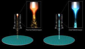
Conventional “thermal field emission” (TFE) eBeam systems operate at more than 1,500°C. Physicists have been working for decades to commercialize CFE eBeam technology because the lower temperature results in a narrower beam with more electrons, thereby enabling sub-nanometer image resolution and a 10X increase in imaging speed. Until now, CFE technology has not been stable enough for commercial applications because impurities inside the system accumulate on the eBeam emitter and degrade the flow of electrons; in TFE systems, these impurities are automatically repelled. Applied has made two breakthroughs that bring CFE eBeam systems into high-volume manufacturing:
- Extreme ultra-high vacuum eBeam columns: Applied has developed unique eBeam columns that house the eBeam emitter and other critical components. The new CFE columns combine an extreme ultra-high vacuum operating environment along with specially developed chamber materials that greatly reduce the presence of contaminants. Special pumps help achieve a vacuum of well below 1x10-11 millibar, which is two to three orders of magnitude better than for TFE systems and close to the vacuum found in outer space.
- Novel self-cleaning mode: Even under extreme ultra-high vacuum, tiny amounts of residual gas can form in the eBeam column. If a single atom adheres to the eBeam source tip, it can partially block the emission of electrons, resulting in unstable operation. Applied has developed a cyclical self-cleaning process that continuously removes contaminants from the CFE source, thereby enabling stable and repeatable performance.
“The commercialization of CFE is the biggest advance in eBeam imaging technology in decades,” said Keith Wells, Group Vice President of Imaging and Process Control at Applied Materials. “With the industry’s highest resolution and electron density, Applied’s new CFE technology allows chipmakers to quickly detect and image defects they’ve never been able to see before.”
Introducing SEMVision® G10 and PrimeVision® 10
Applied today introduced its first two eBeam systems based on CFE technology.
SEMVision G10 Defect Review System: Applied’s SEMVision product family is the most advanced and widely used eBeam review system in the world, enabling customers to image the smallest defects to understand the issues impacting chip process development and high-volume manufacturing. The new SEMVision G10 system uses CFE technology to achieve sub-nanometer image resolution and up to 3X faster imaging than the company’s previous best product. Applied’s SEMVision G10 system has been chosen by all GAA customers as the process development tool of record and has already generated more than $400 million in revenue. SEMVision G10 systems have also been deployed by leading memory customers for developing emerging DRAM and NAND process nodes and ensuring high-volume production of existing memory nodes.
PrimeVision 10 Defect Inspection System: The PrimeVision 10 system is a new addition to Applied’s eBeam product portfolio. The system features nanometer-scale resolution for detecting tiny defects on the surface of wafers, as well as 3D detection technology that finds yield-critical defects buried in 3D GAA structures and high-aspect-ratio memory devices. With its high eBeam density, the PrimeVision 10 system can generate high-resolution images up to 10X faster than TFE-based eBeam inspection systems.
Applied Materials has become the process control industry’s number-one supplier of eBeam systems, with calendar 2021 revenue of more than $1 billion and eBeam market segment share of over 50 percent*.
Additional information about Applied’s CFE technology and new systems will be discussed at the company’s “eBeam Technology and Product Launch” event being held later today.
About Applied Materials
Applied Materials, Inc. (Nasdaq: AMAT) is the leader in materials engineering solutions used to produce virtually every new chip and advanced display in the world. Our expertise in modifying materials at atomic levels and on an industrial scale enables customers to transform possibilities into reality. At Applied Materials, our innovations make possible a better future. Learn more at www.appliedmaterials.com.*Source: TechInsights, April 2022
Contact:
Ricky Gradwohl (editorial/media) 408.235.4676
Michael Sullivan (financial community) 408.986.7977A photo accompanying this announcement is available at https://www.globenewswire.com/NewsRoom/AttachmentNg/c3497496-c198-4454-a546-056b4d7c72fd. This photo is also available at Newscom, www.newscom.com, and via AP PhotoExpress.

Applied Materials’ CFE Technology: the Next-Generation of eBeam Imaging
Operating at room temperature, Applied Materials’ cold field emission (CFE) technology [shown on the right] produces a narrower beam with more electrons, thereby increasing nanoscale image resolution by up to 50% and imaging speed by up to 10X compared to conventional thermal field emission (TFE) eBeam technology [shown on the left].
